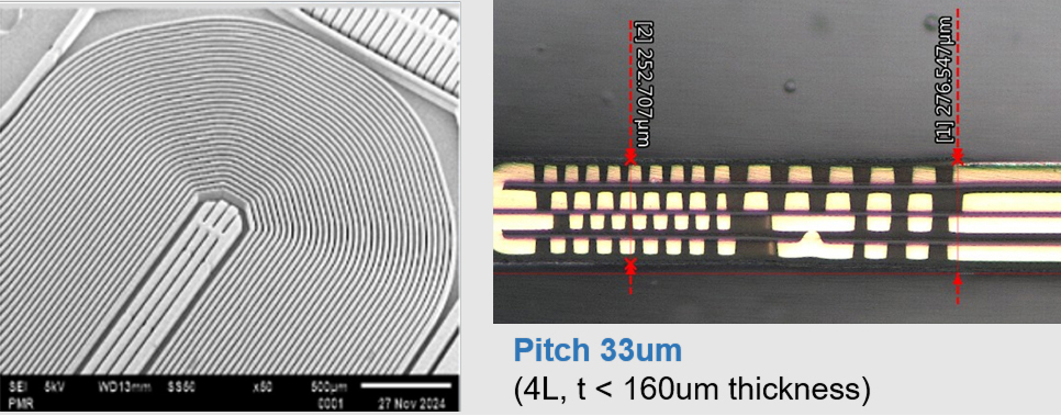
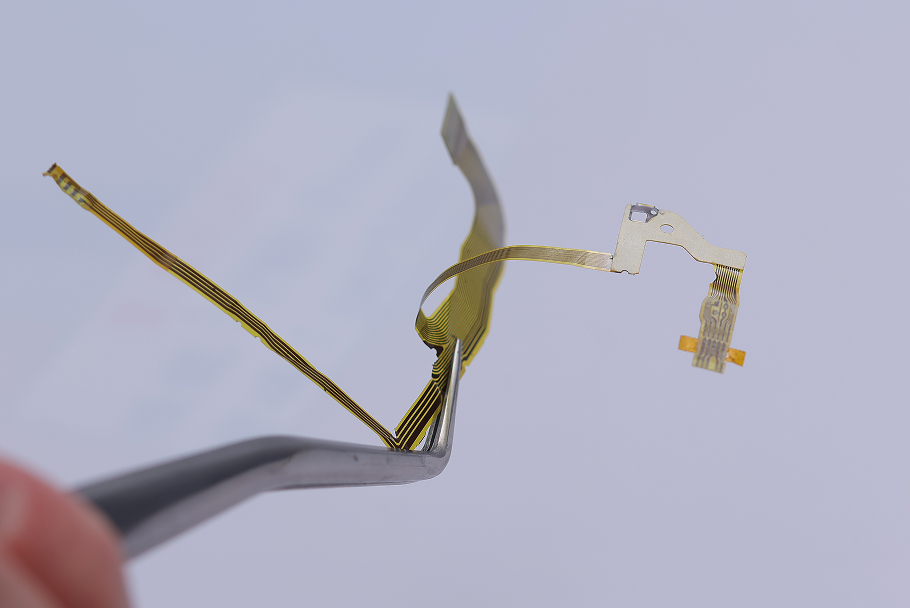
Ultra-Fine-Line Flexes
PMR’s pre-drilling technology can reach via < 25μm, line width/space can reach 10/10μm, which can be used for high-density circuit designs.
● Capabilities
| Min Line / Space (um) |
25/25 | 15/15 | 10/10 |
|---|---|---|---|
| Trace Height (um) |
4~50 | 2~20 | 1~20 |
| Total pitch variation in 50mm.(%) | < 3% | < 3% | < 3% |
➤ Multi-Layer Flexes
When it comes for multi-layer flex designs, PMR’s semi-additive process (SAP) has more advantages than the traditional subtractive process.
● Characteristics of multi-layer flex technology
- (1) Excellent electrical properties, better heat conductivity and more convenient assembly performance with lightweight substrate film.
- (2) Able to improve the integrity of circuit design.
- (3) Minimizing circuit area and improving the integration of electronic devices.
● Capability : Layer : 3~6 Layers
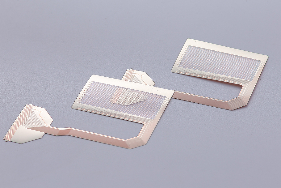
➤ Ultra-Thin Flexes
Ultra-thin flexes are extremely thin and highly flexible printed circuit films, suitable for small space designs and conducive to effectively increasing the utilization rate.
● Features of ultra-fine-line flex technology
- (1) Extremely thin design: Low thickness, suitable for ultra-thin electronic products
- (2) High flexibility: Bendable, foldable, low R angle, suitable for wearable applications with multiple dynamic folds
- (3) Lightweight: Reducing the weight of equipment and improving portability
- (4) High conductivity: Polyimide (PI) and other materials are used to ensure stable current transmission
- (5) High temperature resistance: Suitable for high-temperature environments to improve the reliability of electronic components
●Capabilities
- PI thickness: min. 4μm
- Line thickness: min. 5μm
- Overall thickness: 4-layer total thickness < 50μm
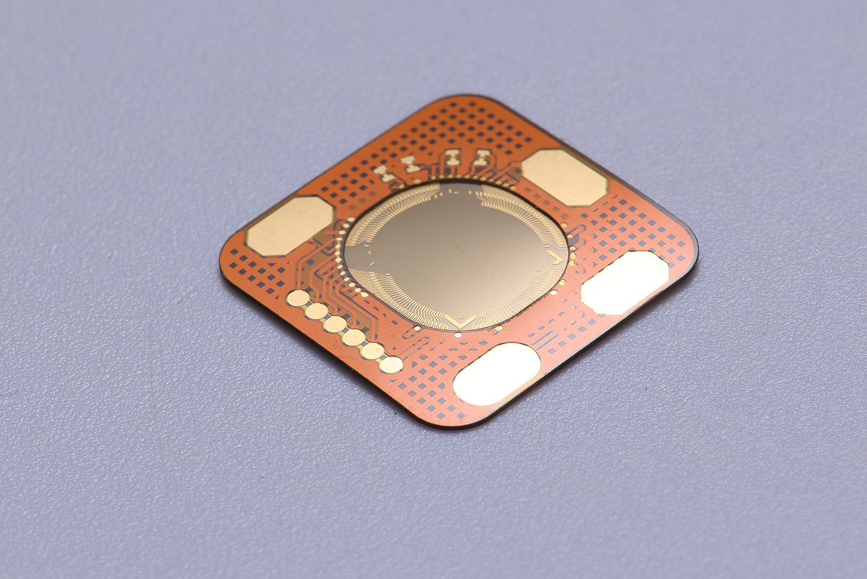
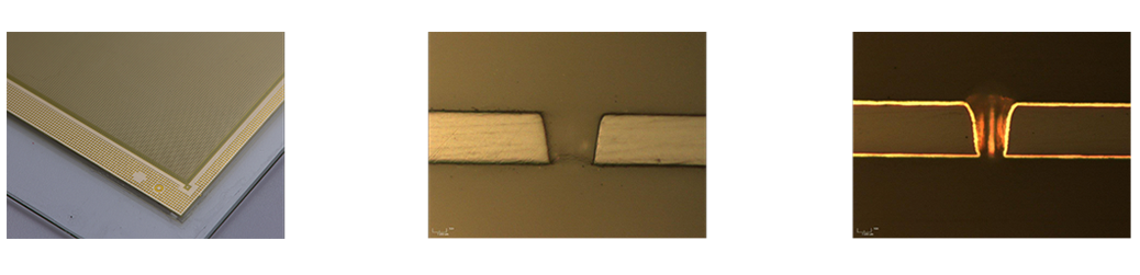
High-Density Microvia Flexes
Fine-line circuit designs are inseparable from the demand for high-density microvias. The pre-drilling technology applied on polyimide (PI) can provide a fast and low-cost process to make microvias (via holes diameter less than 25μm) which can meet the demand of ultra-high-density (20M/m2) microvia products, and is far superior to the drilling process for traditional copper foil substrates (FCCL) in terms of via-hole density and yield.
● Capability
| Through-hole density | VIA Density(VIA/m²) Definition | |
|---|---|---|
| High Density | 500 K/m2 | |
| Super High Density | 5,000 K/m2 | |
| Ultra High Density | 10,000 K/m2 | |
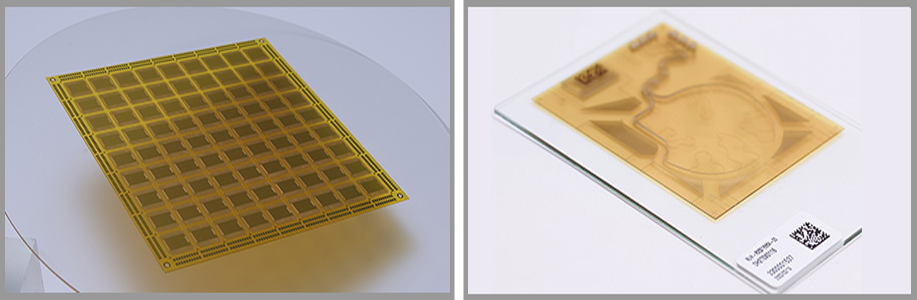
Flex-On-Glass Substrates
Easy-to-bend but thin flexible printed circuit (FPC) is difficult to use in high-precision die packaging (ex. flip chip). Attaching FPC to the glass carrier can solve the control problem of high-precision FPC assembly. After the back-end process is completed, FOG can be easily detached from the glass carrier. FOG (flex-on-glass flexes) can meet the industrial requirements of extreme fineness, thinness, flatness and accuracy, providing the highest precision and high-yield performance for FPC applications.
● Product applicable specifications
- Panel size: 110*75mm ~ 510*515mm
- Lamination accuracy : < 50μm
- Flatness: < 2μm
- Selection of adhesive materials: CDF (cold-debond film)/TDF (thermal-debond film, pyrolytic glue)